AI-translated from the Chinese original View original
It had been a while since I last built something new. I recently remembered the Nixie displays in Metro 2033, which I played years ago. Their Cold War-era, Soviet clock-shop aesthetic left a lasting impression. The glowing digits inside glass tubes have a distinctive character, and I had wanted to make a Nixie device of my own ever since.
A series of Codex usage-limit resets gave me an opportunity to start. The PCB design demonstration released with GPT 6 Astra in September 2026 had also stuck with me. I decided to try building a small desktop device that would use Nixie tubes to display my remaining token allowance, and see how far AI could take a hardware idea toward a physical object. Spending spare AI quota to build a quota display seemed fitting, putting AI to work on its own allowance.
Before starting, I set one rule for the project.
I would make every change to the design files by describing what I wanted to the agent.
As the human in the loop, I would define requirements, choose between options, inspect the results, and validate the assembled hardware. Feedback from each stage would guide the next round.
I called the project Nixie Indicator. This first article covers the circuits, PCB, enclosure, and hardware bring-up. Firmware, the desktop companion, and the presentation video follow in the next two articles.
Choosing the Design
Codex and I worked incrementally, using spec-driven development. I started with rough notes on the idea and candidate approaches, then wrote a project overview and roadmap covering the goals, modules, and order of work. We refined the design in stages, recording agreed interfaces and constraints in formal design documents. Updating those documents alongside the implementation gradually gave the project an organized engineering context.
To help the agent understand my development and project-management habits, I also gave it my earlier custom keyboard and Techno Keyer projects as references. Providing existing projects was an important way to shape its context. Concrete examples communicated my preferred organization and design conventions and reduced repeated explanations.
The main components gradually settled into place.
-
Nixie tubes. Two DGM01 tubes provide the two-digit display.
-
MCU. An ESP32-S3, which I had used in several other projects, retrieves data over Wi-Fi.
-
LCD. A small screen provides metric names, units, status, and settings. The idea came from the CWO networked Morse-code desk device I had bought from its maker, Xifengzui.
-
USB-C. One connector handles both 5 V power and firmware flashing.
-
Rotary encoder. A side-mounted knob handles selection and confirmation.
I chose DGM01 tubes after watching Sadudu revive Nixie-tube manufacturing in China by making them himself. I admired the work and wanted to use his tubes in my own project.
I split the main electronics into two stacked boards for three reasons.
-
Separate the high- and low-voltage areas. The display board contains the high-voltage supply and Nixie drivers. The control board holds the MCU, USB interface, and low-voltage supply.
-
Reduce the desktop footprint. Stacking the boards saves horizontal space.
-
Allow future variants. A different display board could accommodate tubes such as the Soviet IN-18 while reusing as much of the control board as possible.
The upper display board carries the two tubes. Two sets of headers connect it to the lower control board for low-voltage power and control signals. The LCD sits vertically on a separate front board.

Circuit Design
Power Supply
I settled on a single 5 V USB-C input. One branch feeds an AMS1117-3.3 regulator for the MCU, display logic, and LCD. The other passes through a controlled switch to an off-the-shelf high-voltage module on the display board.
The high-voltage module is the XGGF-HV-tiny from Acorn Workshop, a supplier recommended by Sadudu. I designed the downstream circuits around its nominal output of approximately 170 V, concentrating on the interface, enable control, and mounting space. Startup behavior and operation with both tubes connected would be checked on the actual hardware.
The low-voltage input switch, module enable, and display blanking are controlled separately. Startup follows this sequence.
-
Keep the outputs blanked while preparing the display data.
-
Switch on the low-voltage input branch, then enable the high-voltage module.
-
Release blanking to display the digits.
The boards share a common ground. Their physical separation provides no electrical isolation. I included a separate discharge path for the high-voltage supply and enclosed the pins and solder joints. Residual voltage can remain after the display goes dark and needs to be measured separately.

Driving the Nixie Tubes
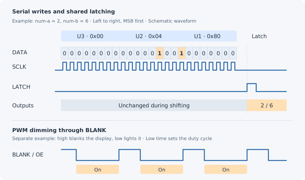
The two tubes have twenty digit cathodes in total. Three 74HC595 shift registers expand the outputs, and twenty MMBTA42 high-voltage transistors switch the individual cathodes. Each tube has its own anode current-limiting resistor.
The ESP32 sends serial data and latches the outputs together. Four of the twenty-four available shift-register outputs are unused. Normal operation selects one digit per tube.
Brightness is controlled by PWM on the shared blanking signal. The final frequency was chosen by comparing results on the assembled board.
PCB Design
I started with component placement, establishing functional areas, positions, and assembly relationships before routing. Getting the overall arrangement right made the connections easier to plan and reduced the need to move large groups of components during routing.
Component Placement
The first layouts quickly showed that functional requirements and connectivity were insufficient on their own. The agent’s initial placement was fairly arbitrary. I had to specify grid alignment, functional grouping, proximity between related components, and space between modules.
After a round or two, the placement began to meet my expectations. Decoupling capacitors, interface protection, and driver resistors needed to sit near their associated connections. I also asked the agent to place equivalent driver transistors according to the actual tube pin positions, then revise the schematic channel assignments to suit their positions relative to the 74HC595s. The wiring could follow the physical layout, with firmware generating display data using the final mapping.
The stacked structure introduced another set of constraints. Both main boards face upward, so components on top of the control board face components on the underside of the display board. An apparently empty area in a two-dimensional layout could sit directly below a high-voltage module or connector in the assembled device. Tube centers, inter-board connectors, and mounting holes also had to stay aligned across the boards.

Routing Iterations
Routing was substantially more complex than placement and took more time. I saw plenty of awkward traces and changes that solved one problem while creating another. A route could look reasonable locally and still fit poorly into the board as a whole. I gradually stopped expecting a perfect first pass. Words like “reasonable,” “tidy,” and “compact” were insufficient. I needed to inspect the board, identify specific problems, and iterate with Codex.
The first scripts focused on individual connections. The overall layout included unnecessary detours, unexpected right angles and acute corners, and other awkward paths. A round took roughly half an hour, with considerable token consumption. I could watch my Pro 100 weekly allowance slowly falling as the iterations continued.

KiCad’s text-based project files let an agent read and modify component coordinates, nets, and traces. We gradually established a repeatable process.
Read. Use project files and design documents to understand placement and routing constraints.
Modify. Adjust component positions and generate routing paths with Python scripts.
Check. Run rule checks and export images for my review before continuing.
Routing became a geometry and path-planning problem, reducing the amount of individual clicking and dragging in the GUI.
I recorded recurring issues as explicit routing rules.
-
Keep related traces parallel where possible, with consistent bends and fewer short fragments or pointless reversals.
-
Prefer same-layer connections and avoid repeated vias merely to shorten a local route.
-
Apply the appropriate constraints to high-voltage nets, power, and ordinary signals. Convenient connectivity should never depend on indiscriminately reducing trace widths or clearances.
Another effective change was to work in stages on local areas. Finishing one group of related components and connections before routing shared signals and power was easier to control than repeatedly revising the whole board. Confirmed areas were retained where possible, and each new change was checked for its effect on existing connections and return paths.
According to my rough notes, it took about ten rounds for routing to approach the intended result. Script execution and automated visual checks eventually fell below ten minutes per round. I still inspected the paths and assembly relationships, while recurring rules were incorporated into the scripts for subsequent iterations.
KiCad’s design rule checking (DRC) was valuable throughout. Explicit trace-width and clearance requirements, checked after each round, exposed unconnected nets and routing violations introduced by the agent and constrained unintended changes.
I also checked the two boards together, including connector alignment and mounting positions, and kept components and metal structures on the opposite board clear of high-voltage areas. The side-mounted encoder affected the upper board as well. Its installed height and position required an edge cutout, followed by adjustments to nearby components and traces.
Enclosure and Assembly Design
Once the PCBs took shape, I used a three-dimensional assembly to check component heights, connector fit, and assembly clearances. Interference that was difficult to see in two dimensions became much clearer. Uncertain bends and fit allowances still needed confirmation with real parts.
Many common components can reuse the 3D models supplied with KiCad footprints. For unusual parts such as Nixie tubes, supplying the necessary datasheets and dimensions was enough for the agent to produce models that worked surprisingly well.
Board dimensions and spacing evolved during layout and assembly design. I wanted a compact device with enough room for components and connectors between the boards. The tubes sit on top, the screen faces forward, USB faces backward, and the knob projects from the right side. The resulting enclosure is 3D-printed in black PA12S. The upper shell includes the complete front frame, while the lower shell wraps around the bottom, sides, and rear.
I wanted a seamless front and no exposed top fasteners. The board assembly therefore mounts inside the upper shell, with enclosure seams along the sides, rear, and underside.

I worked through the fasteners layer by layer using section views. Mounting posts inside the upper shell contain heat-set inserts. Short screws secure the front of the display board, while brass standoffs clamp the rear, creating four suspension points. The rear standoffs also maintain the board spacing and accept the lower-shell screws at their lower ends. The board mounting and lower-shell attachment are independent, so removing the lower shell leaves the upper shell and electronics together.
I then checked screw engagement through each layer, clearance to blind-hole bottoms, and tool access. Reinforcement at the mounting-post roots also had to leave a clear insertion path for the lower shell. Section views let me evaluate those relationships together.
For example, the inter-board connectors and front-board cable can remain connected during enclosure removal, but the projecting encoder restricts how the lower shell can move. After removing the knob and external retaining hardware, the lower shell needs a slight tilt and translation to clear the shaft, rear USB connector, and support posts. Assembly design needs to cover insertion and removal as well as the final fit.

With design documents and assembly models available, having the agent produce an assembly manual was straightforward. Fastener relationships, assembly order, and precautions already had a documented basis. Model views turned those decisions into illustrated instructions. The same models later supported the presentation video, whose materials and camera work are covered in the companion article.
Assembly and Bring-up
JLCPCB manufactured the boards and assembled the basic components. After delivery, I hand-soldered the remaining parts and fitted the Nixie pin sockets. My first check was for shorts with a multimeter. I then tested the modules progressively before assembling the high-voltage display board, tubes, and other main parts for full-device bring-up.
An unexpected issue during dimming
After the tubes were working, I noticed a faint noise at some brightness settings and compared several PWM frequencies. Overall, 500 Hz worked best. The noise became noticeably quieter at 100% brightness.
At 5 kHz it became more obvious. At 16 kHz the noise disappeared, but brightness control became much less effective. At 25 kHz dimming clearly failed. I kept 500 Hz. The exact source of the noise has yet to be confirmed by measurement.

Reflections
The project showed me how far AI’s hardware engineering capabilities have progressed. PCB design still required repeated refinement, especially routing. Connectivity was only the beginning, and tidy paths and practical assembly took further work. Given clear requirements, specifications, and rule checks, the agent could nevertheless perform a substantial amount of detailed design.
Its three-dimensional understanding surprised me even more. Datasheet dimensions were enough to create usable models for simple parts. Enclosure splits, board suspension, and assembly clearances could all be developed through discussion. Based on this project, I feel its spatial understanding and modeling already exceed those of most people. The progression from dimensions to models and then to relationships between parts was more mature than I expected.
In this collaboration, AI increasingly felt like an extension of my hands. An octopus can coordinate its arms through higher-level intent without directing every movement individually. Likewise, I could express a design intention and have the agent carry out the detailed operations. My preferences and aesthetic judgment still shaped the result. I remained involved through requirements, inspection, and physical testing, even though every file change went through the agent.
AI brought a substantial productivity improvement to this kind of hardware project. Previously, similar work could occupy weeks of personal time, starting with simulation and verification and progressing through gradual refinement. Now, two or three concentrated days, plus sustained token consumption, can potentially bring the main design to a manufacturable stage. Simulation, checks, and physical verification remain necessary, while drawing, modeling, and repeated revisions take much less time. An idea that starts in spare time has a better chance of becoming a physical device.
Part 2 covers firmware and the desktop companion, including how the device retrieves quota information and turns it into glowing digits.
Last modified on 2026-11-05